- 您现在的位置:买卖IC网 > Sheet目录3882 > PIC18F4539T-I/ML (Microchip Technology)IC MCU FLASH 12KX16 EE A/D 44QFN
2002 Microchip Technology Inc.
Preliminary
DS30485A-page 131
PIC18FXX39
16.3.6
SLAVE MODE
In Slave mode, the data is transmitted and received as
the external clock pulses appear on SCK. When the
last bit is latched, the SSPIF interrupt flag bit is set.
While in Slave mode, the external clock is supplied by
the external clock source on the SCK pin. This external
clock must meet the minimum high and low times, as
specified in the electrical specifications.
While in SLEEP mode, the slave can transmit/receive
data. When a byte is received, the device will wake-up
from SLEEP.
16.3.7
SLAVE SELECT
SYNCHRONIZATION
The SS pin allows a Synchronous Slave mode. The
SPI must be in Slave mode with SS pin control enabled
(SSPCON1<3:0> = 04h). The pin must not be driven
low for the SS pin to function as an input. The Data
Latch must be high. When the SS pin is low, transmis-
sion and reception are enabled and the SDO pin is
driven. When the SS pin goes high, the SDO pin is no
longer driven, even if in the middle of a transmitted
byte, and becomes a floating output. External pull-up/
pull-down resistors may be desirable, depending on the
application.
When the SPI module resets, the bit counter is forced
to ‘0’. This can be done by either forcing the SS pin to
a high level or clearing the SSPEN bit.
To emulate two-wire communication, the SDO pin can
be connected to the SDI pin. When the SPI needs to
operate as a receiver, the SDO pin can be configured
as an input. This disables transmissions from the SDO.
The SDI can always be left as an input (SDI function),
since it cannot create a bus conflict.
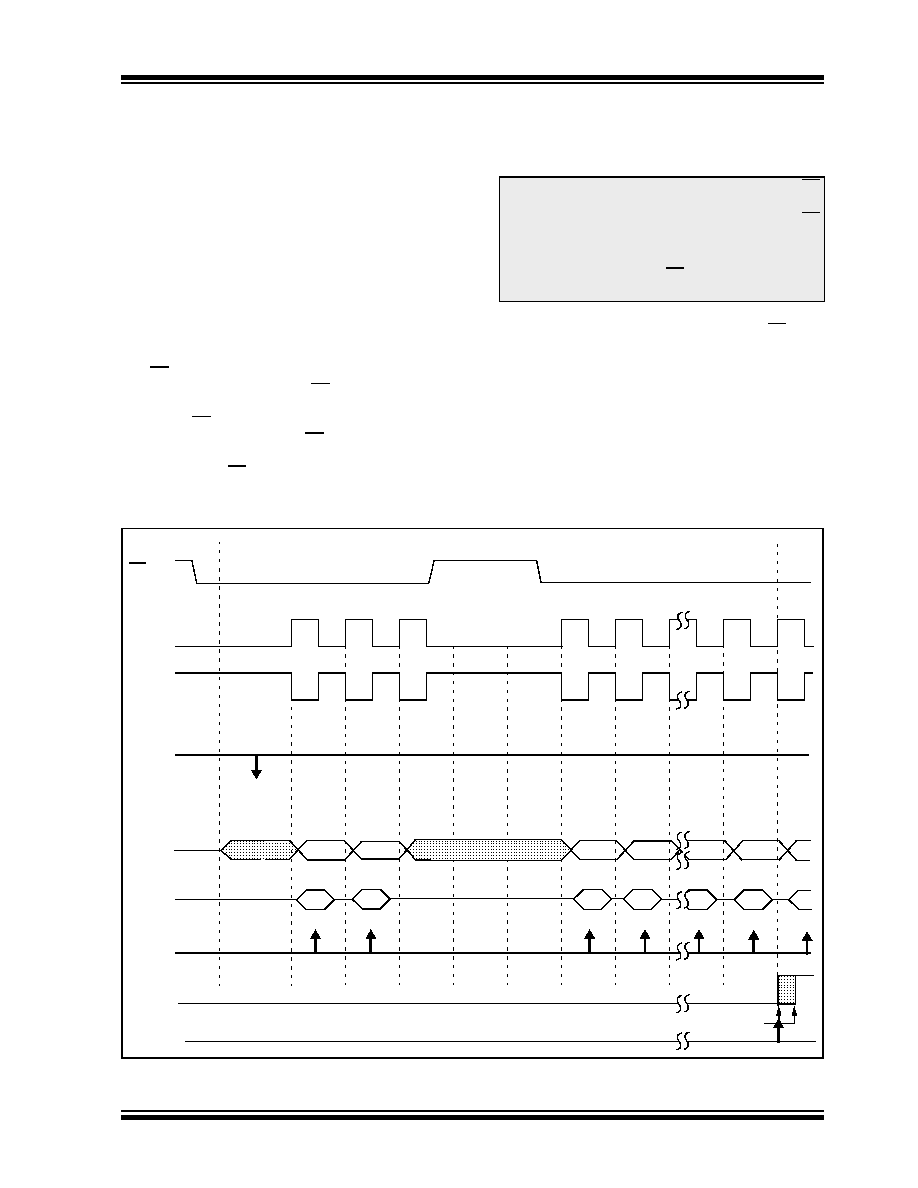
FIGURE 16-4:
SLAVE SYNCHRONIZATION WAVEFORM
Note 1: When the SPI is in Slave mode with SS
pin control enabled (SSPCON<3:0> =
0100
), the SPI module will reset if the SS
pin is set to VDD.
2: If the SPI is used in Slave mode with CKE
set, then the SS pin control must be
enabled.
SCK
(CKP = 1
SCK
(CKP = 0
Input
Sample
SDI
bit7
SDO
bit7
bit6
bit7
SSPIF
Interrupt
(SMP = 0)
CKE = 0)
(SMP = 0)
Write to
SSPBUF
SSPSR to
SSPBUF
SS
Flag
bit0
bit7
bit0
Next Q4 cycle
after Q2
↓
发布紧急采购,3分钟左右您将得到回复。
相关PDF资料
PIC18LF2539T-I/SO
IC MCU FLASH 12KX16 EE AD 28SOIC
PIC18LF4539T-I/PT
IC MCU FLASH 12KX16 EE AD 44TQFP
PIC16LF874AT-I/ML
IC MCU FLASH 4KX14 A/D 44QFN
PIC16F77T-E/ML
IC MCU FLASH 8KX14 A/D 44QFN
PIC16F874A-E/ML
IC MCU FLASH 4KX14 A/D 44QFN
PIC16F74T-I/ML
IC MCU FLASH 4KX14 A/D 44QFN
PIC16F77T-I/ML
IC MCU FLASH 8KX14 A/D 44QFN
PIC18F24K20-I/SS
IC PIC MCU FLASH 8KX16 28SSOP
相关代理商/技术参数
PIC18F4539T-I/PT
功能描述:8位微控制器 -MCU 24KB 1408 RAM 32 I/O RoHS:否 制造商:Silicon Labs 核心:8051 处理器系列:C8051F39x 数据总线宽度:8 bit 最大时钟频率:50 MHz 程序存储器大小:16 KB 数据 RAM 大小:1 KB 片上 ADC:Yes 工作电源电压:1.8 V to 3.6 V 工作温度范围:- 40 C to + 105 C 封装 / 箱体:QFN-20 安装风格:SMD/SMT
PIC18F4550EPT
制造商:Microchip Technology Inc 功能描述:
PIC18F4550-I/ML
功能描述:8位微控制器 -MCU 32kBF 2048RM FSUSB2 RoHS:否 制造商:Silicon Labs 核心:8051 处理器系列:C8051F39x 数据总线宽度:8 bit 最大时钟频率:50 MHz 程序存储器大小:16 KB 数据 RAM 大小:1 KB 片上 ADC:Yes 工作电源电压:1.8 V to 3.6 V 工作温度范围:- 40 C to + 105 C 封装 / 箱体:QFN-20 安装风格:SMD/SMT
PIC18F4550-I/P
功能描述:8位微控制器 -MCU 32kBF 2048RM FSUSB2 RoHS:否 制造商:Silicon Labs 核心:8051 处理器系列:C8051F39x 数据总线宽度:8 bit 最大时钟频率:50 MHz 程序存储器大小:16 KB 数据 RAM 大小:1 KB 片上 ADC:Yes 工作电源电压:1.8 V to 3.6 V 工作温度范围:- 40 C to + 105 C 封装 / 箱体:QFN-20 安装风格:SMD/SMT
PIC18F4550-I/PT
功能描述:8位微控制器 -MCU 32kBF 2048RM FSUSB2 RoHS:否 制造商:Silicon Labs 核心:8051 处理器系列:C8051F39x 数据总线宽度:8 bit 最大时钟频率:50 MHz 程序存储器大小:16 KB 数据 RAM 大小:1 KB 片上 ADC:Yes 工作电源电压:1.8 V to 3.6 V 工作温度范围:- 40 C to + 105 C 封装 / 箱体:QFN-20 安装风格:SMD/SMT
PIC18F4550T-I/ML
功能描述:8位微控制器 -MCU 32kBF 2048RM FSUSB2 RoHS:否 制造商:Silicon Labs 核心:8051 处理器系列:C8051F39x 数据总线宽度:8 bit 最大时钟频率:50 MHz 程序存储器大小:16 KB 数据 RAM 大小:1 KB 片上 ADC:Yes 工作电源电压:1.8 V to 3.6 V 工作温度范围:- 40 C to + 105 C 封装 / 箱体:QFN-20 安装风格:SMD/SMT
PIC18F4550T-I/PT
功能描述:8位微控制器 -MCU 32kBF 2048RM FSUSB2 RoHS:否 制造商:Silicon Labs 核心:8051 处理器系列:C8051F39x 数据总线宽度:8 bit 最大时钟频率:50 MHz 程序存储器大小:16 KB 数据 RAM 大小:1 KB 片上 ADC:Yes 工作电源电压:1.8 V to 3.6 V 工作温度范围:- 40 C to + 105 C 封装 / 箱体:QFN-20 安装风格:SMD/SMT
PIC18F4553-I/ML
功能描述:8位微控制器 -MCU 32KB FLSH 2048 RAM FSUSB 2.0 12B ADC RoHS:否 制造商:Silicon Labs 核心:8051 处理器系列:C8051F39x 数据总线宽度:8 bit 最大时钟频率:50 MHz 程序存储器大小:16 KB 数据 RAM 大小:1 KB 片上 ADC:Yes 工作电源电压:1.8 V to 3.6 V 工作温度范围:- 40 C to + 105 C 封装 / 箱体:QFN-20 安装风格:SMD/SMT